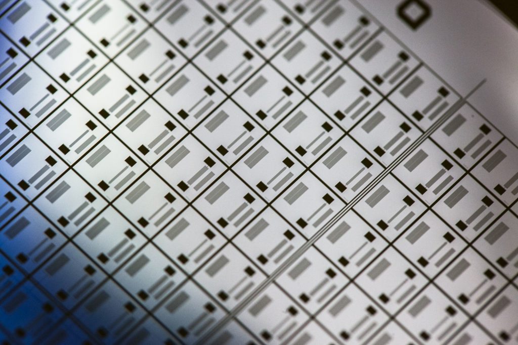
Dry etching (ion plasma):
- RIE, DRIE
- FIB (Focus Ion Beam)
- Materials: Silicon (max 6 inches), Glass, Si3N4, LiNbO3,… (max 4 inches)
Wet etching:
- KOH, BHF
- Vapor HF Etching
Dry etching (ion plasma):
Wet etching:

In addition tosiliconetching, we have developed various deep etching processes for dielectric materials in a clean room:
| Engraved materials | Depth |
Verticality of the sides |
Roughness at the bottom of the engraving |
| Glass | Up to 200 µm | 70° to 100 µm | Ra < 500nm |
| Quartz | Up to 200 µm | 85° to 100 µm | Ra < 10nm |
| Lithium niobate | Up to 10 µm | 75° to 10 µm | Ra < 10nm |
Benefits:
– Collective etching of micrometric resolution patterns with depths of up to a hundred microns
–New features for your devices
–Improved performance of your devices
Different applications are targeted:
– Structuring of microfluidic channels in biocompatible materials (Glass, etc.)
– Manufacture of optical waveguides in electro-optical materials (Lithium Niobate …)
– Engraving of piezoelectric materials for radiofrequency devices (Quartz, etc.)
The development of these processes has received financial support from the Region Bourgogne Franche-Comté.
contact : florent.bassignot@femto-engineering.fr

UV & electronic lithography Photolithography mask manufacturing

Deposition of thin and thick layers

Precision cutting Lapping & polishing Wire bonding Wafer bonding Micro-assembly (flip-chip)

Microscope (MEB, optic, FIB), mechanical profilometer Specific measures : material constraints, optical index, contact angle
Femto Engineering | From science to society
15B avenue des Montboucons, 25030 Besançon Cedex – France
Subscribe to our newsletter to receive all our news directly