- Manufacturing of PPLN / PPLT crystals
- Components PPLN ridge

Wafer Hybrid
– Multi-material metallic bonding
– Multi-material thinning
– Multi-material thin layers
Fields :
We manufacture of custom PPLN structures We offer in particular the inversion of the domains on a niobate and lithium tantalate wafer as well as the cutting and polishing of the guides.
Specifications :
| Type of conversion | SHG / SFG / DFG / SPDC |
| Wavelength | 750 nm – 3500 nm |
| Poling period | > 10 µm |
| Chip | On request |
| Anti-Reflective coating | On demand |
PPLNs are widely used in non-linear optics, in particular for manufacturing frequency conversion components.
We have developed a component based on our technologies for high efficiency frequency conversion applications (SHG, SFG, DFG).
We propose the modeling of the structure according to your specifications in order to establish the operating points as well as the custom manufacturing of the structure.
Specifications :
| Type of conversion | SHG / SFG / DFG / SPDC |
| Wavelength | 750 nm – 3500 nm |
| Power limitation | ~ 1 W CW |
| Efficiency (SHG) | > 100%W-1cm-2 |
| Length | 5 mm -40 mm |
| Anti-Reflective coating | On demand |
| Packaging / Pigtailing | On demand |

– Multi-material metallic bonding
– Multi-material thinning
– Multi-material thin layers

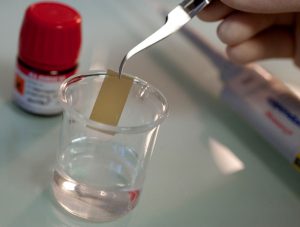
– Manufacturing of chips with plasmonic properties (SPR)
– Specific coatings (SiO2, TiO2, etc)
– Biofonctionnalization
Femto Engineering | From science to society
15B avenue des Montboucons, 25030 Besançon Cedex – France
Subscribe to our newsletter to receive all our news directly