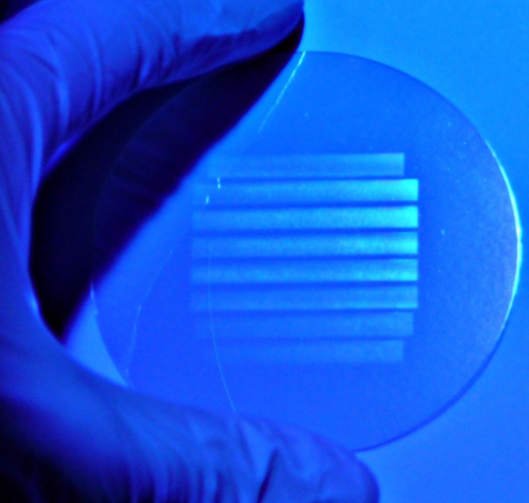
We have developed a specific technology allowing to obtain thin monocrystalline custom layers transferred on plates of diameter up to 4 inches.
Our innovative manufacturing process has many advantages such as the conservation of the properties of materials and the modularity of stacks by the choice of materials (crystals, metals or polymers), their thicknesses (from a few microns to several hundred microns) and of their bonding interfaces (metallic or insulating).
Our custom hybrid substrates
Thin monocrystalline films on electrode or insulator

SPECIFICATIONS
- Wafer size: from sample to 4 inch diameter plates
- Useful surface > 98%
- Bonding strength > 25MPa
- Layer thickness: from 1µm to a few hundred microns.
- Number of layers in the stack: 1 to 10
APPLICATIONS
- Radio-Frequency: Resonators, sensors, filters…
- Photonics: laser, electro-optical sensors…
- MEMS: actuator, sensor…


